



What is a glass substrate? How does it differ from ordinary substrates?
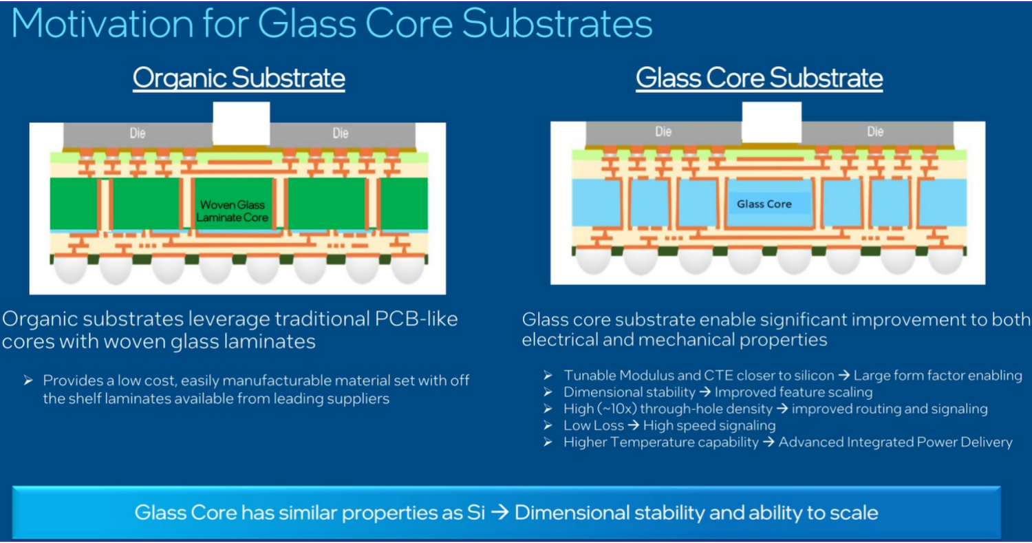
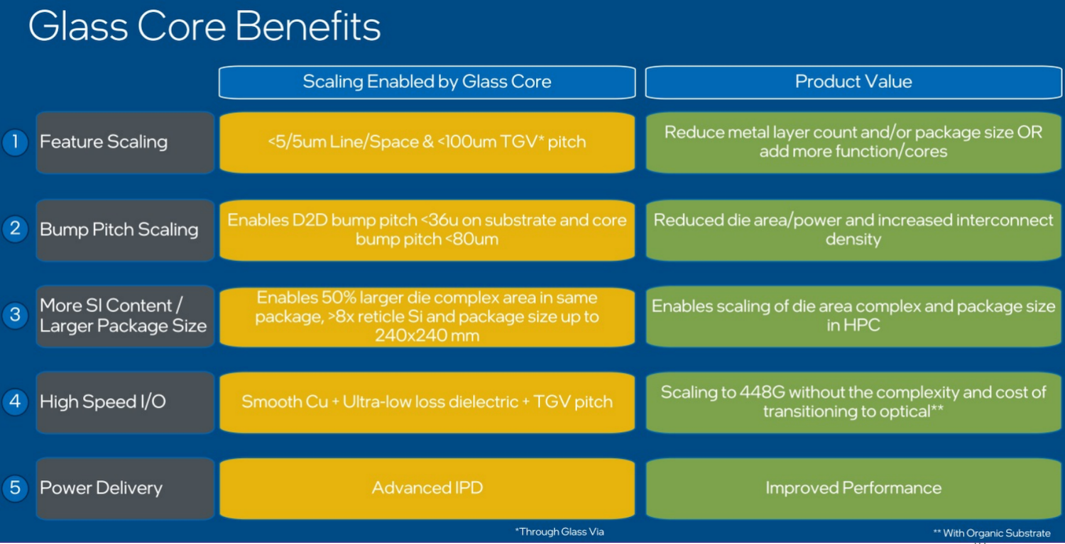
A glass substrate replaces traditional plastic substrates. It enables the formation of finer circuits, and features excellent heat resistance and bending resistance, which facilitates large-scale commercial application.
Restricted by inherent physical properties, conventional substrate materials consume more power and are prone to expansion and warpage. In contrast, glass substrates are better suited to meet future industry demands.
Why have glass substrates become a high-profile technology?
As Moore’s Law gradually approaches its limit, semiconductor manufacturers are shifting from 2D to 3D architecture. By adopting chip stacking and advanced packaging technologies, the industry continues to increase transistor counts for enhanced performance, making packaging a critical link in the process. Amid this trend, Intel has unveiled the industry’s first glass substrate designed for advanced packaging, breaking traditional technical constraints, with mass production scheduled between 2026 and 2030.
What glass packaging substrate products does Side offer?
A wafer refers to a silicon chip used for the fabrication of silicon semiconductor integrated circuits. Various circuit components and structures can be processed on silicon wafers to produce integrated circuits with specific electrical functions.
Leveraging proprietary etching technologies and advanced processing techniques, Side maintains strict geometric tolerance control. Its high-precision ultra-thin structured glass wafers are applicable to high-precision and high-accuracy components. Custom thickness solutions are available within an ultra-thin thickness range to meet customized production requirements.
